本文共 8040 字,大约阅读时间需要 26 分钟。
SPI主机实现
一、硬件层
(1)外部引线
SPI通信的最小结构为一主一从结构,主机向从机提供信号发送接收时钟SCLK。主机与从机之间存有四根引线,即MOSI(主收从发)、MISO(主发从收)、SCK(通信时钟)、CS(从机片选信号)。其中,通过在主机上增加片选信号输出端的数目,或引入编码,译码结构可以使得主机控制更多的从机,实现一主多从的SPI通信。本设计中默认为一主一从最小结构。
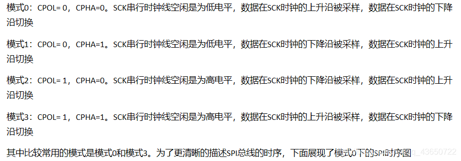
(2)四种工作模式
SPI通信协议规定了4钟工作模式,在实际应用中应当保证主机和从机工作在相同的工作模式下。SPI工作模式通过时钟极性CPOL和时钟相位CPHA联合指定。其中CPOL指定SCK在空闲状态时的电平,CPHA指定在SCK的何种边缘进行数据采样。其标识如下:

二、FPGA代码实现
(1)思路
SPI模式0主机控制器在SCK上升沿时对数据进行采样。由于在时钟上升沿进行数据采样,那么,接收/发送状态机的状态应当早于SCK时钟上升沿提前准备好接收/发送状态,也就是说在低电平期间就需要准备好
对于发送状态机,由于数据在SCK时钟的下降沿进行状态变换,又因为从机在上升沿采样,因此选择在SCK的低电平中心将需发送的数据压至MOSI线上。
对于接收状态机,同样采用SCK下降沿进行状态跳变。接收状态机在SCK上升沿时将数据采集至接收缓冲口,并在采集完一字节数据后生成信号标志脉冲。
对于SPI主机控制器,另一个重要的模块是控制模块,它是用来生成SCK时钟与CS片选信号的模块。由于本文设计只有一个从机,因此只单纯的控制CS的电平。SCK时钟的生成也是依靠状态机,其机理为当状态机处于IDLE空闲状态时,检测到读/写请求,在时钟相位变为下降沿时进入工作状态,并输出8个完整的SCK时钟。此后,状态机转入STOP状态,并在一个周期内检测是否有新的请求信号到来,若无抵达空闲状态,若有,转入工作状态。
(2)代码实现
宏定义文件
//// Company: NanJing University of Information Science & Technology// Engineer: Yang Cheng Yu// // Create Date: 2020/01/13 20:01:50// Design Name: spi_master// Module Name: global_define// Project Name: SPI2// Target Devices: // Tool Versions: // Description: // // Dependencies: // // Revision:// Revision 0.01 - File Created// Additional Comments:// //`define SCK_PEDG (phase==9'd499)//默认使用100KHZ的频率,50M/100k = 500`define SCK_HIGH (phase==9'd124)`define SCK_NEDG (phase==9'd249)`define SCK_LOW (phase==9'd374)
控制模块
`include "global_definition.v"//// Company: NanJing University of Information Science & Technology// Engineer: Yang Cheng Yu// // Create Date: 2020/01/13 20:01:50// Design Name: spi_master// Module Name: control_module// Project Name: SPI2// Target Devices: // Tool Versions: // Description: // // Dependencies: // // Revision:// Revision 0.01 - File Created// Additional Comments:// //module control_module( input clk, input rst, output reg sck, output reg cs_n, output reg[8:0] phase, input wr_req, input rd_req, output reg[3:0] cnt//位数计数器); reg[1:0] state; reg[1:0] next_state; localparam IDLE=2'b00; localparam WORK=2'b01; localparam STOP=2'b11; always@(posedge clk or negedge rst)begin if(!rst) phase <= 9'd0; else if(phase==9'd499) phase <= 9'd0; else phase <= phase + 1'b1; end //状态机状态转移逻辑 always@(posedge clk or negedge rst)begin if(!rst) state <= IDLE; else if(`SCK_NEDG) state <= next_state; else state <= state; end //状态组合判断 always@(wr_req or rd_req or cnt)begin case(state) IDLE: if(wr_req||rd_req) next_state <= WORK; else next_state <= IDLE; WORK: if(cnt==4'd8) next_state <= STOP; else next_state <= WORK; STOP: if(wr_req||rd_req) next_state <= WORK; else next_state <= IDLE; default: next_state <= IDLE; endcase end //状态机输出 always@(posedge clk or negedge rst)begin if(!rst)begin sck <= 1'b0; cs_n <= 1'b1; cnt <= 4'd0; end else begin case(state) IDLE:begin sck <= 1'b0; cs_n <= 1'b1; cnt <= 4'd0; end WORK:begin cs_n <= 1'b0; if(`SCK_PEDG)begin sck <= 1'b1; cnt <= cnt + 1'b1; end else if(`SCK_NEDG) sck <= 1'b0; else sck <= sck; end STOP:begin cnt <= 4'd0; sck <= 1'b0; cs_n <= 1'b1; end default:begin cnt <= cnt; sck <= sck; cs_n <= cs_n; end endcase end endendmodule
发送模块
`include "global_definition.v"//// Company: NanJing University of Information Science & Technology// Engineer: Yang Cheng Yu// // Create Date: 2020/01/13 20:01:50// Design Name: spi_master// Module Name: spi_tx// Project Name: SPI2// Target Devices: // Tool Versions: // Description: // // Dependencies: // // Revision:// Revision 0.01 - File Created// Additional Comments:// //module spi_tx( input clk, input rst, input wr_req, input [7:0] data_wr, input [8:0] phase, output reg wr, output reg mosi, input [3:0] cnt); reg[1:0] state; reg[1:0] next_state; localparam IDLE=2'b00; localparam WORK=2'b01; localparam STOP=2'b11; //状态机状态转移 always@(posedge clk or negedge rst)begin if(!rst) state <= IDLE; else state <= next_state; end //状态组合判定 always@(wr_req or cnt)begin case(state) IDLE: if(wr_req) next_state <= WORK; else next_state <= IDLE; WORK: if(cnt==4'd8) next_state <= STOP; else next_state <= WORK; STOP: if(wr_req) next_state <= WORK; else next_state <= IDLE; default: next_state <= next_state; endcase end //状态机输出 always@(posedge clk or negedge rst)begin if(!rst)begin mosi <= 1'b0; wr <= 1'b1; end else begin case(state) IDLE:begin mosi <= 1'b0; wr <= 1'b1; end WORK:begin wr <= 1'b0; //由于上升沿采样,所以在上升沿到来前把数据给到MOSI if(`SCK_LOW)begin case(cnt) 4'd0:mosi <= data_wr[7]; 4'd1:mosi <= data_wr[6]; 4'd2:mosi <= data_wr[5]; 4'd3:mosi <= data_wr[4]; 4'd4:mosi <= data_wr[3]; 4'd5:mosi <= data_wr[2]; 4'd6:mosi <= data_wr[1]; 4'd7:mosi <= data_wr[0]; default:mosi <= 1'b0; endcase end end STOP:begin wr <= 1'b1; mosi <= 1'b0; end default:begin wr <= wr; mosi <= mosi; end endcase end endendmodule
接收模块
`include "global_definition.v"//// Company: NanJing University of Information Science & Technology// Engineer: Yang Cheng Yu// // Create Date: 2020/01/13 20:01:50// Design Name: spi_master// Module Name: spi_rx// Project Name: SPI2// Target Devices: // Tool Versions: // Description: // // Dependencies: // // Revision:// Revision 0.01 - File Created// Additional Comments:// //module spi_rx( input clk, input rst, input rd_req, output reg[7:0] data_rd, input[8:0] phase, output reg rd, input miso, input[3:0] cnt); reg[1:0] state; reg[1:0] next_state; localparam IDLE=2'b00; localparam WORK=2'b01; localparam STOP=2'b11; //状态机状态转移 always@(posedge clk or negedge rst)begin if(!rst) state <= IDLE; else state <= next_state; end //状态组合判定 always@(rd_req or cnt)begin case(state) IDLE: if(rd_req) next_state <= WORK; else next_state <= IDLE; WORK: if(cnt==4'd8) next_state <= STOP; else next_state <= WORK; STOP: if(rd_req) next_state <= WORK; else next_state <= IDLE; default: next_state <= next_state; endcase end //状态机输出 always@(posedge clk or negedge rst)begin if(!rst)begin rd <= 1'b1; data_rd <= 8'b0000_0000; end else begin case(state) IDLE:begin rd <= 1'b1; data_rd <= 8'b0000_0000; end WORK:begin rd <= 1'b0; if(`SCK_PEDG)begin//下降沿采样 case(cnt) 4'd0:data_rd[7] <= miso; 4'd1:data_rd[6] <= miso; 4'd2:data_rd[5] <= miso; 4'd3:data_rd[4] <= miso; 4'd4:data_rd[3] <= miso; 4'd5:data_rd[2] <= miso; 4'd6:data_rd[1] <= miso; 4'd7:data_rd[0] <= miso; default:data_rd <= data_rd; endcase end else data_rd <= data_rd; end STOP:begin rd <= 1'b1; data_rd <= data_rd; end default:begin rd <= rd; data_rd <= data_rd; end endcase end endendmodule
顶层模块及例化
//// Company: NanJing University of Information Science & Technology// Engineer: Yang Cheng Yu// // Create Date: 2020/01/13 20:01:50// Design Name: spi_master// Module Name: spi_master// Project Name: SPI2// Target Devices: // Tool Versions: // Description: // // Dependencies: // // Revision:// Revision 0.01 - File Created// Additional Comments:// //module spi_master( input clk, input rst, input miso, output mosi, output sck, output cs_n, output wr, output rd, input[7:0] data_wr, output[7:0] data_rd, input wr_req, input rd_req); wire[8:0] phase; wire[3:0] cnt; control_module control_module( .clk (clk), .rst (rst), .sck (sck), .cs_n (cs_n), .phase (phase), .wr_req (wr_req), .rd_req (rd_req), .cnt (cnt)//位数计数器); spi_tx spi_tx( .clk (clk), .rst (rst), .wr_req (wr_req), .data_wr (data_wr), .phase (phase), .wr (wr), .mosi (mosi), .cnt (cnt)); spi_rx spi_rx( .clk (clk), .rst (rst), .rd_req (rd_req), .data_rd (data_rd), .phase (phase), .rd (rd), .miso (miso), .cnt (cnt));endmodule
RTL视图
 状态机图
状态机图 
发表评论
最新留言
关于作者